Description
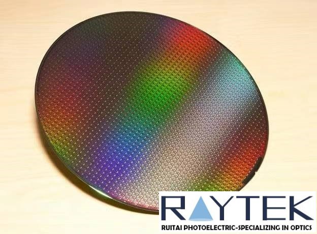
Product Description:The starting material of the wafer is silicon. Silica ore is refined by electric arc furnace, chlorinated with hydrochloric acid, and distilled to produce high-purity polysilicon with a purity of 99.999999999%. The polycrystalline silicon is melted, seed crystals are planted in the molten liquid, and then slowly pulled out to form a cylindrical monocrystalline silicon ingot. Since the silicon ingot is a seed crystal whose crystal plane orientation is determined It is gradually formed in the molten silicon raw material, and this process is called "crystal growth". The silicon ingot is then cut into sections, rolled, sliced, chamfered, polished, laser engraved, and packaged to become silicon wafers, which are "wafers".

Main Cooperation Materials Manufacturers:
CORNING, OHARA, SCHOTT, LEONI, AGC,HELLMA, NIKON,VITRON,C-LASER,ETC
Main Export Countries & Areas:
Usa, Uk, Japan, Germany, Spain, France, Swiss, Korea, Russia, Pakistan, India, Portugal, Canada, New Zealand, Australia, Saudi Arab, Turkey, Finland, Poland ,etc.
Raytekoptics Extra value added services offered:
1). Optical workcraft & process solution design;
2). Rough processing raw materials;
3). Semi finishing raw materials;
4). Fabricate custom sizes and shapes;
5). Design and supply custom coatings;
6). Modify and resurface customer supplied materials;
7). Drill holes, notch glass and provide beveled substrates;
8). Precision polish optics with non-standard aspect ratios;
Payment Method: by T/T or Western Union.
Delivery time: 7-10 days.
Quality Warranty: Ruitaiphotoelectric(Raytekoptics) offers quality warranty for our optics products with "3R" policy. For any inferior-quality products, Ruitaiphotoelectric(Raytekoptics) is responsible for return, replacement and refund.


